Cost of bug – Learnings for verification engineer
Everyone related to any form of ASIC design verification has to internalize one fact: the “cost of bug” discovered increases exponentially as it advances in…
Everyone related to any form of ASIC design verification has to internalize one fact: the “cost of bug” discovered increases exponentially as it advances in the ASIC verification phase. There is a big cost difference between bug found pre-silicon versus post silicon. Let’s understand what are those phases.
The ASIC verification takes place in various phases planned as a part of verification strategy. Typically they are unit verification, System/SOC verification, FPGA prototyping or/and Emulation and post silicon validation. Hence bugs can be found in any of these phases.
Leaving all complex cost calculations of these phases on the table, let’s just look at the time and effort to debug the bugs found in different stages. This will automatically bring out the cost element and why it’s important to find as many bugs as possible in, as early phase as possible. Let’s first identify what is required for the debug.
The process of debug requires insight into scenarios created and functionality of the design. Getting these insights in different phases requires different level of time and effort. Time and effort varies because of the limited visibility, tools and methods used.
Let’s take a same bug discovered at different phases, what it takes to debug it?
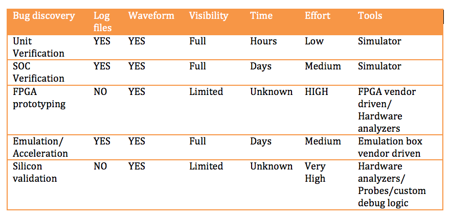
Bugs @ Unit/IP Verification:
Note that when bugs are found in unit simulation, the simulation time is very low. It’s relatively easy and quick to reproduce the issue. There is full visibility through testbench simulation logs and waveforms dumps. With high controllability and observability it’s relatively easy and quick to debug and fix the bugs.
Bugs @ System/SOC Verification:
When the bug is discovered in the SOC simulation, the simulation time is high. Just the SOC test initialization time itself can be comparable to entire largest unit test simulation time. Instead of hours, the waveform generation time can be in days.
Although full dumps can be generated theoretically but there are always practical limitations on tool capacity for handling the bigger designs. To manage it waveforms are generated for limited simulation time and limited hierarchies. This increases the time and effort in root causing the bug.
Everything runs slower, tools will crash periodically and disk space will run out at critical times to add to difficulty.
Bugs @ FPGA Prototyping:
When the same issue is discovered in FPGA prototyping, there is no simulation log to provide the insight in to scenario created. There can be operating system logs or application logs available but they are thousands of miles away from the language design and verification engineers speak.
The waveforms as well are hard to come by. They have to be created through the logic analyzer built in within FPGA for internal signals or through logic/protocol analyzers on interface signals. It will be very limited in visibility.
Many times changing the internal signals captured using FPGA’s internal logic analyzers usage requires re-synthesizing the design. Very limited time waveforms dumps can be captured and requires thoughtful triggers to capture right amount of information. That makes the debug very difficult and time consuming.
Considering the highly iterative nature of capturing information and uncertainty about its availability the time to debug cannot be accurately forecasted.
Bugs @ Emulation:
Although compared to FPGA prototyping the emulation boxes may be lower in speed of operation but offer higher flexibility and greater visibility. They come with their own price tags. The popularity of emulation is growing very fast for the advantages it provides. It has capacity challenges.
Bugs @ Silicon validation:
Now coming to the final form of bug discovery during the silicon functional qualification process. Similar to FPGA prototype debugging there are no log files that clearly provide insight about the scenario similar to simulation logs.
In the FPGA prototyping we can resynthesize and get visibility into some of the internal signals but in silicon debug that possibility also does not exist.
Only the internal debug logic built-in to design can all be relied on. Due to limited capacity only critical internal signals can be routed to debug controller.
Silicon interacts with the real word devices and typically it will be operating at real time speeds. This means capturing interface signals requires special probes, boards, logic and protocol analyzers to gain the visibility. Just to remind, these aren’t free open source tools.
Due to limited visibility the time it takes to root cause bug can become unknown. Also multiple teams have to come together to work together to close on the issue adding to complexity of the debug.
Learnings for verification engineer
Every verification engineer should talk to FPGA prototyping, emulation and silicon bring up and qualification teams. They are also integral part of the functional verification family. Only when we talk to them and hear their stories, it would make simulation based verification engineer feel so lucky. Life seems more abundant in simulation world.
More importantly simulation based verification engineers will realize the price paid in the debug when issues are discovered in later phases of verification. Let’s consider some of the issues and their impact to understand it clearly.
Consider simple bug of the type, power on reset value of control register being set to incorrect value. Bug is simple but it’s impact can be catastrophic. If it happens to be critical pad control signal, it can cause chip or interface to show up as dead. Such simple issue can cost heavily when discovered in the silicon validation.
It can be corner case that shows up after several power state transitions. What we at simulation world think as a lot, happens in real word within split seconds. Now one option here is to disable the low power feature. Disabling that low power feature can make chip to cross the power budgets, making it useless for the targeted application.
Incorrectly waived clock domain crossing path violations escaping the CDC analysis can lead to corruptions of data. It can be nightmare to debug such issues in silicon with very limited visibility as to what is the cause of corruption.
Some issues can also be crazy such as control information appearing as data in data packet activating the control paths inadvertently.
Just remember these issues will have to be debugged under serious time pressure as the silicon samples have arrived and mass production is being gated by silicon sample qualification. Company futures are at stake.
Key takeaway for simulation verification engineer: Every bug found late during FPGA prototyping or silicon validation should at least contribute to learning and building process to minimize its occurrence in future. In order to do that following are some of the guidelines to be considered.
- Simulation-based verification teams have to find ways to catch bugs caught by the FPGA prototyping, Emulation and silicon qualification teams
- Every bug found later is slip in simulation based verification and it should be closely looked into as to why it has happened. Don’t just address that very specific case but look at what is the broader implication of the bug
- Expand bug’s complete scope to make enhancements to the testbench and test suites. Widen the checks and functional coverage around the area where the bug has been found. It may be likely that this is start and there could more hiding behind. This is the right way to verify bug fixes
- It’s equally important to share it with teams who also have similar potential risks. A link layer issue found in the USB could have similar implication for PCIe or UniPro
- Any issues that crept in due to cross team interactions make sure to set up the expectations in executable form. For example analog designs requiring control from digital logic such as pads, PLLs etc. can put the assertions on their interface to make sure the correct power on values are programmed and only legal values are programmed instead of just passing these as requirements
- When the bug is discovered late in game, simulation team should not wait quietly. It makes sense to take proactive approach to help prove or disprove some of theories the debug teams are coming up. Start reviewing constraints, test cases, checks and coverage around the suspected areas. Increase the seeds and get those additional regressions started. Any help provided to quickly reproduce the issue in the simulation based verification environment could be a big help. This is where good testbench architecture would ease the process of recreation and enhancement
Bottom line, make sure every issues found in silicon validation or FPGA prototyping or emulation are addressed in the simulation based verification. Its extremely important to not to repeat the same mistake.